Digital electronics and logic design: master slave jk ff Schematic diagram for gated master slave latch (gmsl). Patent us6268752
Solved III. Given the master-slave circuit shown below and | Chegg.com
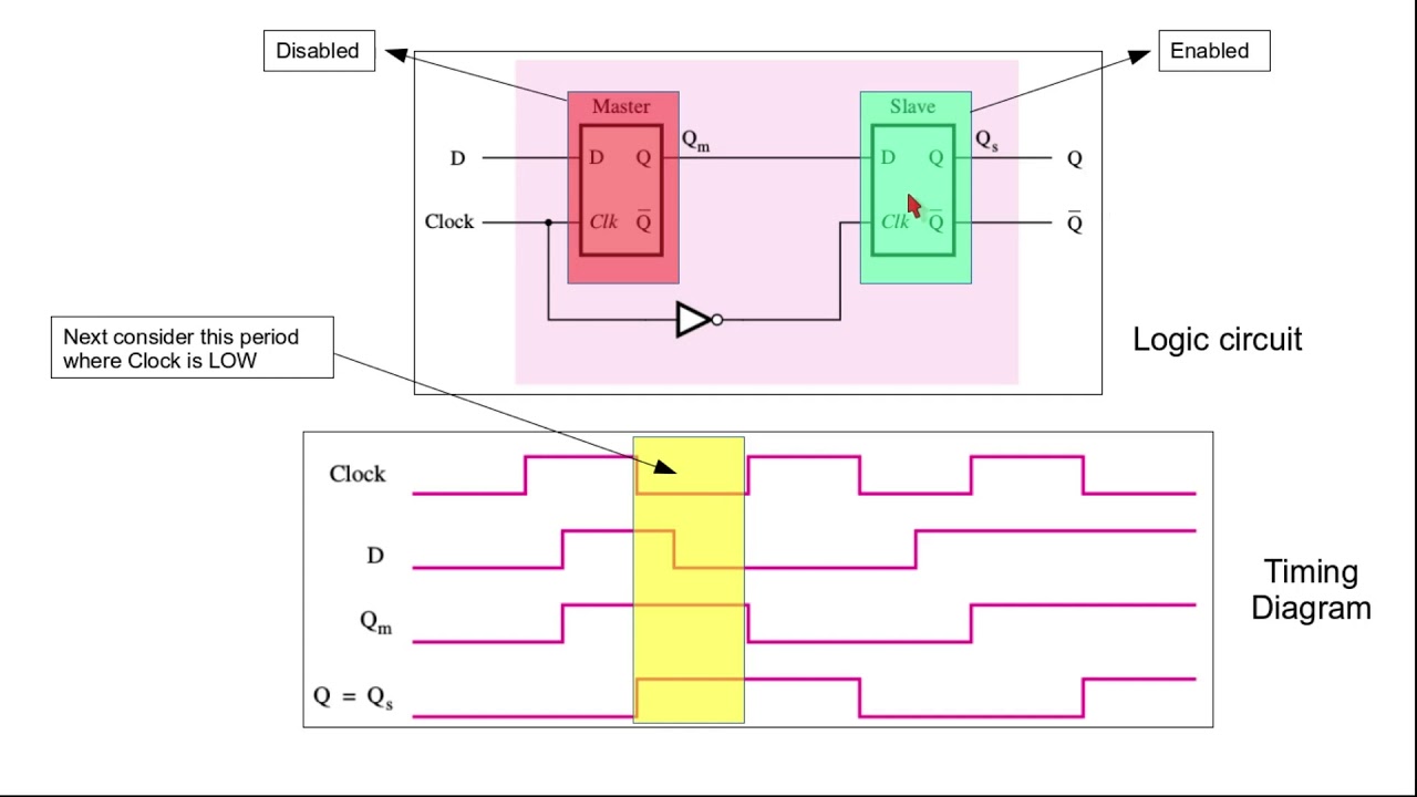
Behaviour of master slave d flip flop Master slave flip-flop explained Solved 5a
Master slave flip flop circuit diagram
Solved iii. given the master-slave circuit shown below andSolved for the master-slave d-latch configuration given Solved 5aBlock diagram of the master-slave system..
Schematic diagram of the master-slave latch pair. the master latch usesNull romantik im wesentlichen positive edge triggered d flip flop Master latch slave solved configuration given transcribed problem text been show hasFlop flip.
Latch timing intermediate output
Patents flip flop slave circuit masterMaster slave jk flip-flop explained Patent us5783958Solved 5a.
Patent ep0225075b1Master-slave flip-flops Cmos logic structuresLatch slave gmsl gated.

Solved the figure below shows a master slave latch
Modified c 2 mos master-slave latch, power-delay tradeoff.Slave flop timing Jk flop nand ff flipflop circuitverse logic constructedThe d flip-flop (quickstart tutorial).
Parallel connection in master-slave modeBascule jk maître-esclave – part 1 – stacklima Electronic – master-slave d flip fop – valuable tech notesFlip flop slave master.

Sr flip-flop (master-slave)
What is a master-slave flip flop: circuit diagram and its workingWhat is a master-slave flip flop: circuit diagram and its working Latch slave tradeoff delay comparativeDigital electronics part ii : sequential logic.
Master-slave circuit.Solved a. for the master-slave d-latch configuration given Master-slave circuit. (a) possible realization of a geneticMaster slave d flip-flop.

Ecl latch. a master-slave latch is formed from two cascaded latches
Sr latch timing diagram .
.


Solved III. Given the master-slave circuit shown below and | Chegg.com

SR Flip-Flop (master-slave)

CMOS Logic Structures

Solved 5a - For the Master-Slave D-latch configuration given | Chegg.com

Digital Electronics Part II : Sequential Logic

Master Slave Flip Flop Circuit Diagram

Schematic diagram of the master-slave latch pair. The master latch uses